
Description

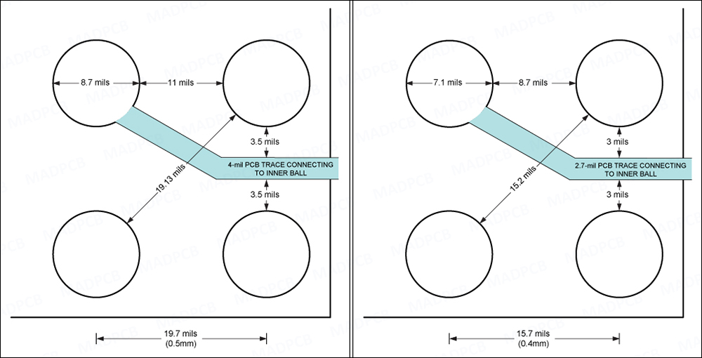
PCB Design Considerations and Guidelines for 0.4mm and 0.5mm WLPs

PCB Review Request] Review for prototype PCB built around MAX86171
Pitch: SMD Pitch, IC Pitch - PCB Design, Fab & Assembly

Test board layout of a single layer FR4 board (5 cm 2 7 cm) with daisy
PCB Design Rules for Chip-on-Board Layout
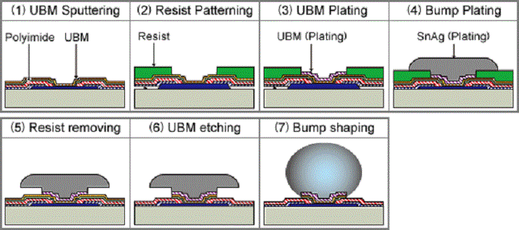
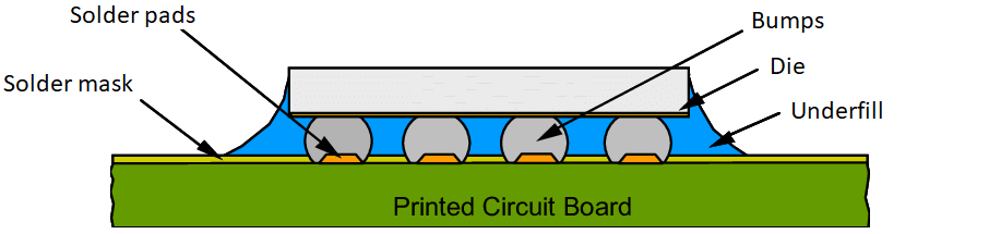
Bump on Pad, Wafer Process Technology

PCB Pads - MorePCB

PCB pad design principles
pub.mdpi-res.com/jlpea/jlpea-11-00002/article_depl
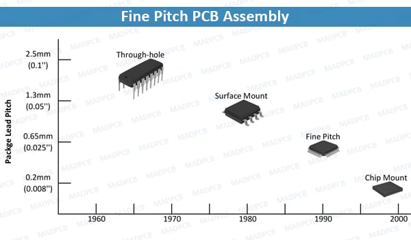
Fine Pitch Technology (FPT): PCB Board Assembly

RDL and Flip Chip Design

What is Pad to Pad (PP) ?
Related products


$ 5.50USD
Score 4.8(517)
In stock
Continue to book
$ 5.50USD
Score 4.8(517)
In stock
Continue to book
©2018-2024, farmersprotest.de, Inc. or its affiliates