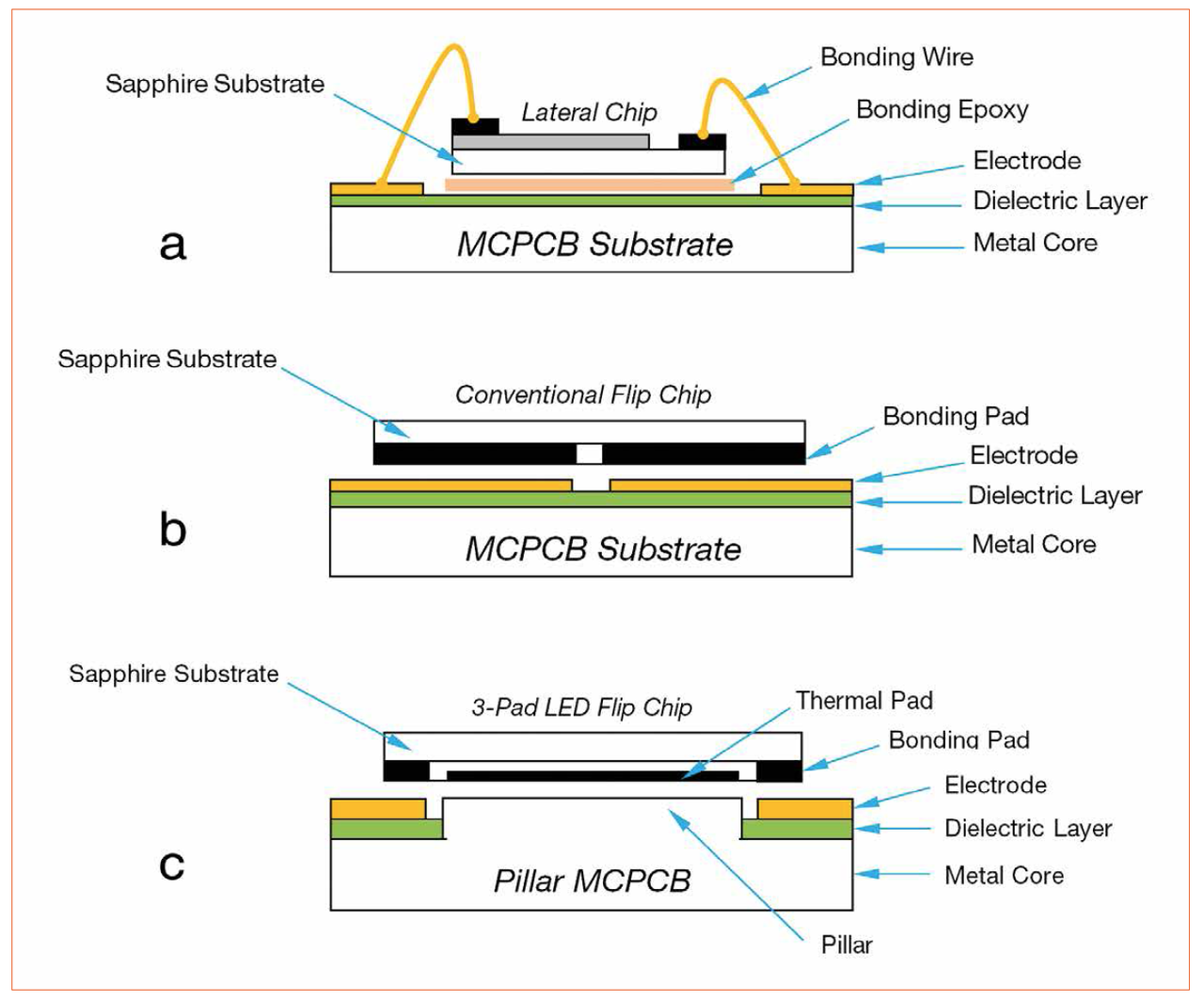
At the University of Alberta, the Imaging Science Lab aims to develop vertically-integrated (VI) CMOS image sensors with capabilities that exceed those of conventional CMOS image sensors. VI-CMOS image sensors are examples of 3D electronics because they consist of photodetectors that are placed in a layer above standard CMOS circuits. Although metal lines commonly pass over transistors in CMOS image sensors, a distinguishing characteristic of VI-CMOS image sensors is the layering of semiconductor devices. The main advantage of vertical integration is that the different layers may be fabricated using different processes, each one optimized to best suit the type of devices it contains.

Die Bonding, Process for Placing a Chip on a Package Substrate

Flipchip bonding.
Soft ionic liquid multi-point touch sensor - RSC Advances (RSC

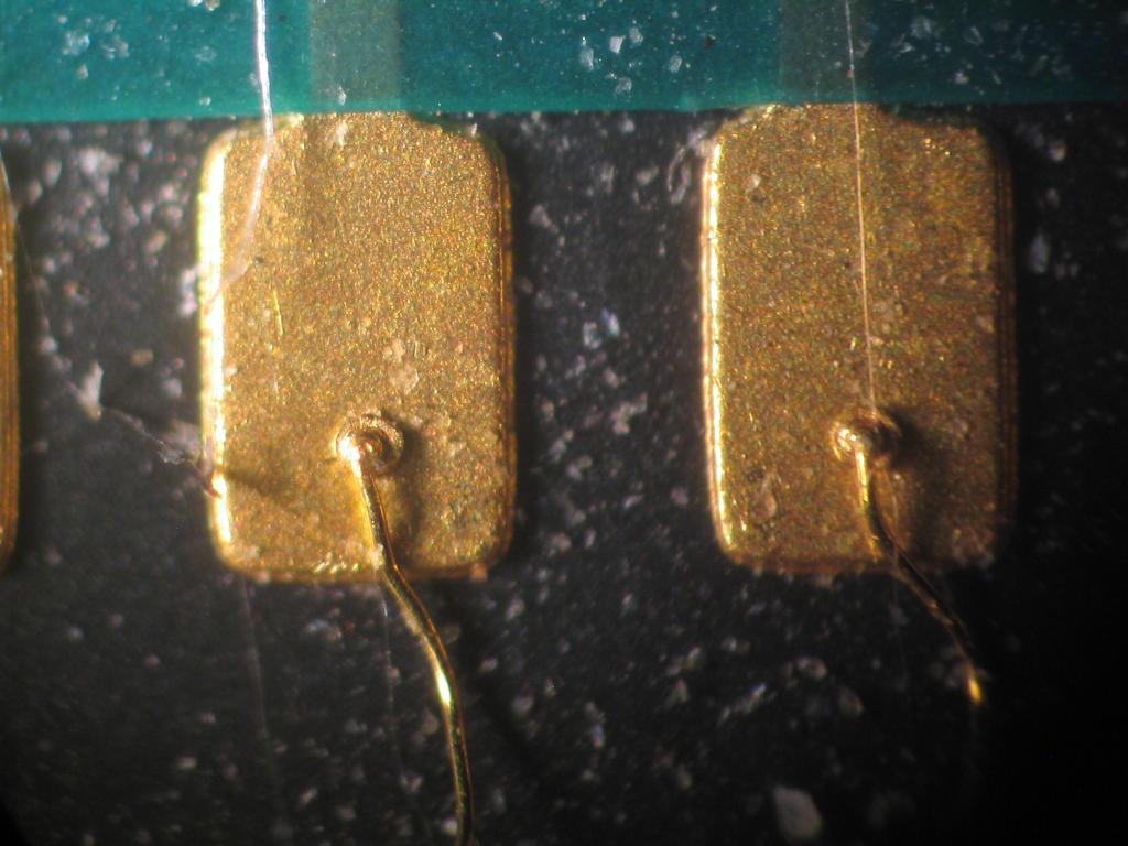
PDF] Design and Fabrication of Bond Pads for Flip-Chip Bonding of
PDF] Design and Fabrication of Bond Pads for Flip-Chip Bonding of

Flip Chip - Chip Scale Package Bonding Technology with Type 7
Flip-Chip

Study of Structure and Failure Mechanisms in ACA Interconnections
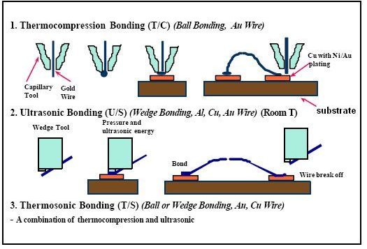
Wire Bonding - The Ultimate Guide Is Here - NextPCB
Micromachines, Free Full-Text
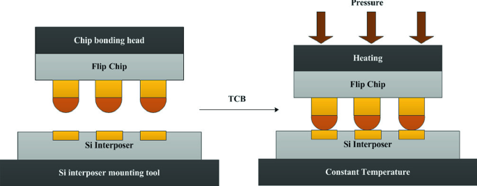
Development of Flip Chip Bonding Process on Silicon Interposer by